Natcore Research & Development Center
On March 2, 2012, Natcore opened its Research & Development Center in Building 308 at Eastman Business Park in Rochester, NY. U.S. Congresswoman Louise Slaughter and Natcore president Chuck Provini wielded the scissors at the ceremonial ribbon cutting. The event was also attended by area political leaders and by members of the Rochester business and professional investment communities.
The facility occupies approximately 20,000 ft2. It houses a laboratory/clean room, a gowning room, administration offices and a warehouse/staging area. The Class 10,000 (ISO 7) clean room uses positive air pressure and a series of filters to eliminate 90% of environmental pollutants (e.g., dust, airborne microbes, aerosol particles and chemical vapors) from outside air. Employees enter and leave through a gowning room, where they don protective clothing such as caps, facemasks, gloves, booties and coveralls. The clean room occupies 8,000 ft2, of which we are actively using about 5,000 ft2 while retaining an opportunity to expand rapidly as needed. We have used this expansion capability in the recent past to add new process equipment without the need to consider a costly space increase or relocation.
The facility has the required equipment and staff to produce and test working solar cells starting from virgin silicon wafers. Development and testing can be done on silicon samples ranging in size from 20 millimeters for one-of-a-kind testing to full industrial size wafers (156mm). In addition, we have the capability to process small experimental variations of one test condition at a time up to low volume pilot processing (100 wafers per hour) for certain of our tools. Here are the main capabilities:
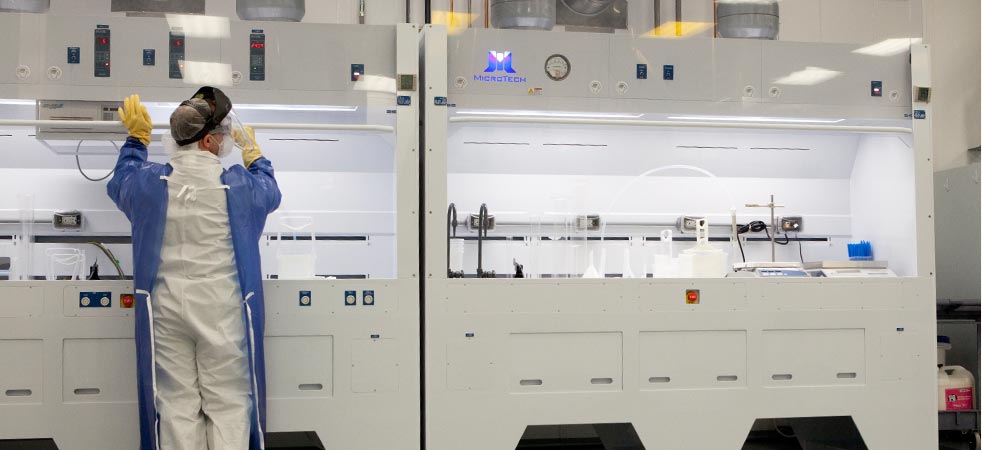
Benchtop Wet Processing (figure 1)
The Natcore Research Facility has two eight-foot cleanroom wet benches provided by Microsystems Technologies (MTS). These benches are equipped with process tanks, sonication equipment, and high purity rinse systems. Our black etch process for light trapping is performed in this area. This equipment is capable of handling up to 12 at a time industry standard 125mm or 156mm square silicon wafers.
Automated Wet Processing / Pilot Volume Tool
(figure 2)
We possess a pilot capacity 12’ wet processing area containing a specialized temperature controlled recirculation tank that is suited to deposition of high density insulating, and can be adapted to other chemistries as needed. The unit also contains large scale temperature controlled tanks, high purity water rinsing systems, and a wafer drier that can be used for up to 50 wafers per batch, permitting throughputs of up to 100 wafers per hour for certain processes.
Diffusion & Thermal Process (figures 3 & 4)
Natcore owns a four-tube Bruce BDF-41 diffusion furnace with 8” diameter tubes and automated sample load/unload. This unit is used for doing industry standard POCl3 diffusions, as well as other thermal treatments including oxidation and forming gas anneal. These processes are important in cell testing and processing.
Contact Application (figures 5 & 6)
A portion of our process is dedicated to applying metal contacts via screen printing. This process line includes a screen printer used for both front and back contact application. We also have a drying oven and a rapid thermal processor (RTP) capable of drying and firing the contacts, respectively.
Deposition Systems:
We have a custom built atomic layer deposition system (ALD) designed to process samples ranging from 20mm x 20mm up to 156mm square standard solar cells. The system can process as much as 12 large samples at a time. We also possess a cryo-pumped vacuum deposition chamber. The chamber is currently capable of physical vapor deposition.
Testing / Analytical (figures 7, 8, & 9)
Natcore has established a number of in-house testing techniques mainly directed toward solar cell characterization. For rapid assessment of our processes, we have charge carrier lifetime measurement and open circuit voltage vs. suns illumination testing. There is also a one-sun illumination system (with uniformity sufficient for 156 mm wafers) that includes current vs. voltage testing electronics, used for finished cell characterization. For electrical properties of the cells, we have equipment to accurately measure contact resistance, and a four-point probe measurement apparatus. Additionally, as part of the Eastman Business Park we have easy access to Eastman Kodak’s analytical technologies division, with a large number of analytical technologies including chemical analysis and properties testing.
(continued below)
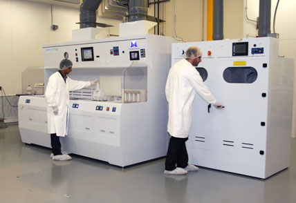
Figure 2: Work performed using customized R&D equipment.
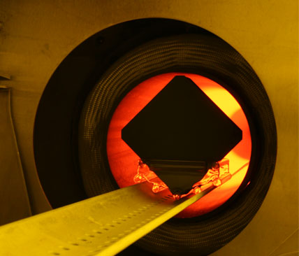
Figure 3: Solar wafers entering the diffusion furnace.
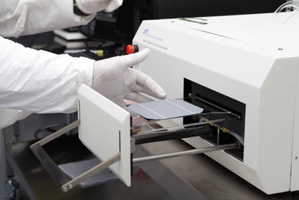
Figure 4: Co-firing of solar cell contacts using a rapid thermal process (RTP)
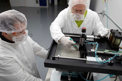
Figure 5: Technicians operating the screen printer to apply grid and back contacts to test solar cells.
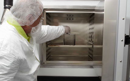
Figure 6: Wafers exiting the drying oven after printing.
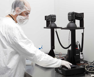
Figure 7: Lifetime measurements to assess passivation performance.
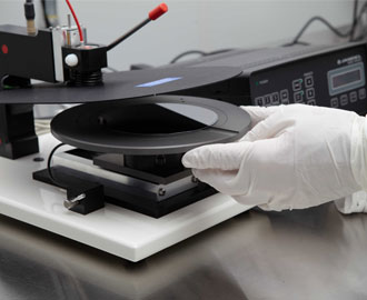
Figure 8: Wafer being placed into the four-point probe to determine emitter sheet resistance or bulk resistivity.
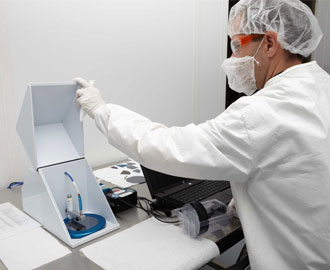
Figure 9: Film thickness measurements using spectral reflectance.
Laser Processing
Natcore has recently acquired a pulsed infrared laser operating at 1064 nm for laser doping of solar cells and formation of all back contact solar cell structures employing a low temperature processes. The laser is capable of a large variety of pulse lengths and powers, and allows for custom temporal shaping of pulses.
We currently have optics permitting spot sizes of around 20-micron diameter as well as other beam shapes. The laser is coupled to a mechanical stage for positioning of the laser exposure with an accuracy of better than five microns. The setup exists in a completely enclosed facility, and is operated from an external control station.